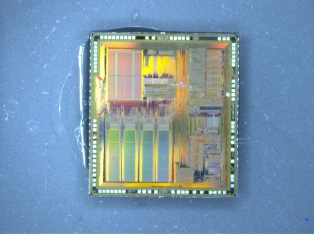
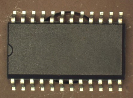
Harvested part after extraction process. All package encapsulant has been removed from die face, edges, and back side.
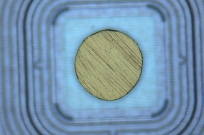
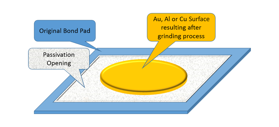
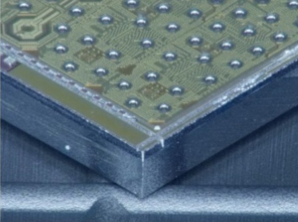
Resulting pads each have a wire-formed, diamond-lapped, planar bonding surface at a uniform height.
Superior Planar Bonding Surface Process
Planar Bonding Surface Process provides a pristine flat surface, suitable for rebond
Best for high reliability applications: ✓ No voids or trapped contaminants; die fully planarized ✓ Same surface area as the original ball or wedge bond ✓ Compatible with Al, Cu wedge bond or Au ball bond ✓ Original bond-to-pad interface remains unchanged
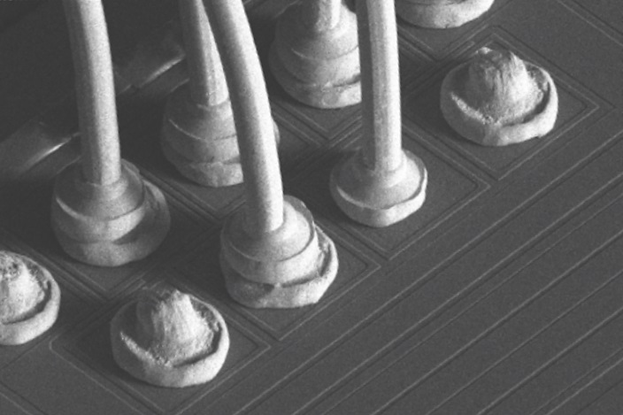
Conventional Ball Bond Removal leaves a remnant of the wire
This will affect long term reliability and performance ✗ Potential for trapped contaminants and non-conformities ✗ Partial surface area contact can increase resistance ✗ Unsuitable for Al wedge bonds
Planar Bonding Surface
Solving Microelectronic Obsolescence
BENEFITS OF DIE EXTRACTION AND REASSEMBLY FOR OBSOLETE IC REPLACEMENT:
Availability: Commercially-plentiful components can be repackaged and retested to mil-aero conditions
Counterfeit risk mitigation: Determining device authenticity is accomplished during extraction
Repackage for harsh environment: High temperature and vibration survivability may require ceramic packages rather than common plastic packages
Time: Redesigning and qualifying a new design can be a prohibitively lengthy process
Cost: The OCM’s minimum lot charge to manufacture an obsolete product can be prohibitively expensive
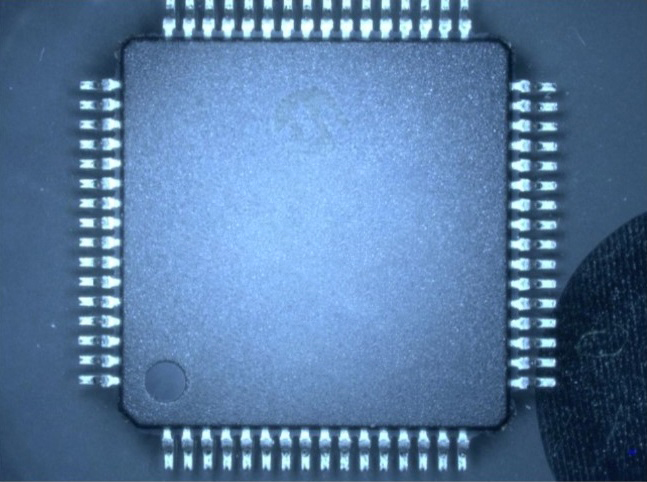
Original part as received
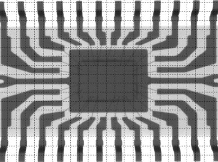
X-Ray of plastic package to determine lead frame locations and pin-outs to die
Initial frontside decap run, to observe chemical compatability to die surface and pads
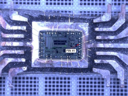
Higher magnification to confirm pin-out and die revision details
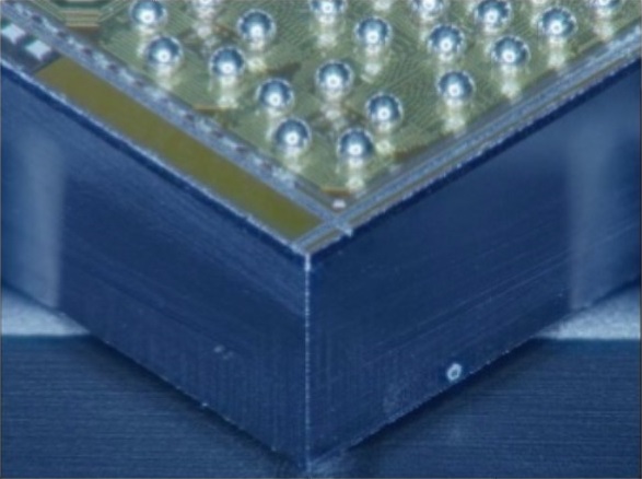
Solder Bump Removal and Die Thinning
Die are received with solder bumps which need to be removed to allow reuse of the die.
Bumps removed. Die shown also thinned to desired customer thickness for repackaging.