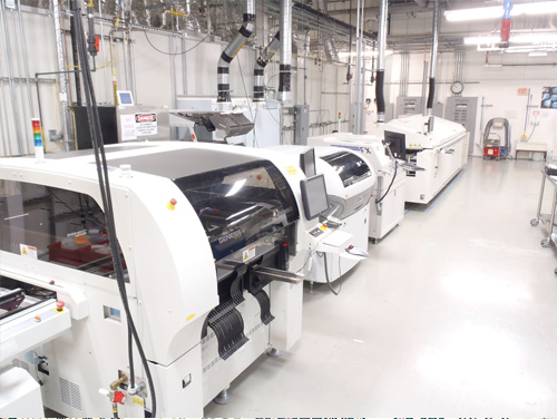
At i3 Microsystems we integrate advanced process and product development with manufacturing to provide wafer level, flip chip and wire bond packaging assemblies from prototype to volume production.
i3 has earned global respect as assembly process experts, enabling customers to increase yields, continually improve processes, and optimize product reliability using our material science and engineering expertise.
Our solutions support the needs of the defense and aerospace, IT, server and super computing and medical markets where highly reliable products built in robust manufacturing operations are essential to success.
Full procurement | Full supply chain | Failure analysis
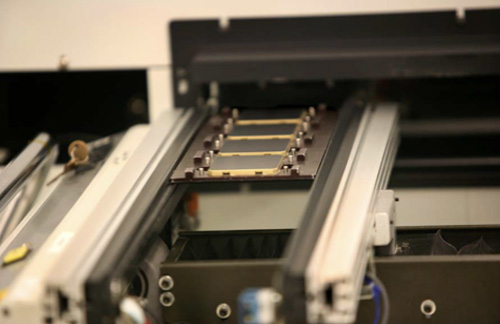
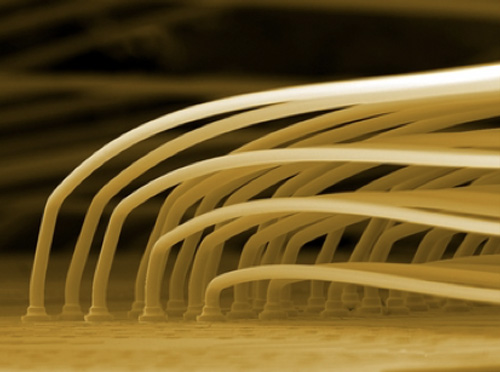
The XY location accuracy of the "free end" of each vertical wire
Repeatable to +/-10μm
The "Z" height of the wire
Repeatable to +/-20μm
System-in-Package and Shrink
Reducing system size, weight, and power (SWaP) is critical to the development of new applications, especially for the defense industry. By achieving reductions in the form factor and power consumption of today’s military and medical electronics, i3 is able to improve mobility and extend operational life, enhancing the overall viability of the product in the marketplace.
Our innovative System-in-Package technology is perfect for the following markets:
Aerospace & Defense
High Performance Computing
Medical
Industrial
i3 has developed system-in-package technology to achieve SWaP goals, bring differentiated products to market quickly and efficiently, and to establish design and supply chain continuity.
Product transferred to Production
Single pass assembly for Hybrid metallurgy: Standard soldered components with lead free die bumps
Package Size: 45 x 45mm, 683μm thick
Substrate: PTFE
X-section 9 layer
50μm vias, 30/35μm Line/space
5348 Flip Chip bumps
728 BGA I/O
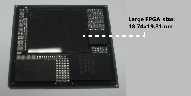
1 very large standard solder Xilinx Flip Chip FPGA
1 RAM
1 Flash Memory
1 Programmable Logic Device with user flash
123 Discrete components placed: 0402 minimum size
Mixed standard solder die attach with lead free SMT components
Functional final test with thermal cycling
Benefits of Utilizing i3’s SiP Technology
Enable more functionality in smaller packages with our organic substrates
Improve electrical performance through a reduction in trace lengths
Simplify, and in many cases eliminate, complex PCB’s all together
Prepackaged IC’s, surface mount components, memory, passives and connectors, while increasing reliability and decreasing weight
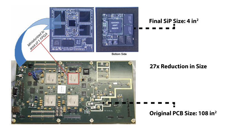
Improve electrical performance, address thermal considerations, provide miniaturization, minimize complexity and achieve size reductions up to 27x or greater
Original PCB Size: 108 in2⇨ Final Sip size: 4 in2
Package Size: 55 x 55mm, 683μm thick
Substrate: Particle filled epoxy
X-section 3-4-3
50μm vias, 30/35μm Line/space
84 ft HDI wiring
>39,000 40 micron UV laser drilled vias
5 Flip Chip FPGA
4 Xilinx FPGA, 3264 I/O w/190μm minimum pitch
Discrete components: 0201 minimum size
638 SMT components placed
Functional final socket & Bed of Nails topside test