To meet our customers’ expectations and applicable regulatory / statutory requirements through delivery of products that reflect continuously improved quality, service, and reliability and maintains the effectiveness of the Quality Management System.
DMEA Accredited Trusted Foundry
ITAR Certified
ISO-9000:2015 Certified
Small Business Enterprise
Class-100 Cleanrooms
HSiP as a FO-WLP Technology
HSiP is capable of simple, single-die, Redistribution Layer (RDL) fabrication
HSIP technology offers tremendous flexibility to accommodate different dietypes, sizes to produce a high performance high density multi-chip packageusing FOWLP.
Process capable to produce a flat HSIP with good electrical circuit whenusing RTV-03 conditions (low bake, longertimes).
** As presented by i3 Microsystems, Inc. at IMAPS2020
Heterogeneous IC Integration
As system performance requirements and complexity continue to grow with an emphasis on SWAP, it is inevitable that heterogeneous IC integration will become the industry standard. The conventional monolithic system on a chip is just not economically feasible to integrate all of the functionality onto one universal technology node. FPGA alone cannot include mixed signal, analog and RF functions as these technologies have vastly diverging requirements. Attempts have been made to combine programmable logic with analog and memory. There is either too little memory, logic or analog performance. These result in a very restricted product offering and as such limit the range of applications that will fit within these constraints. A much more versatile product results from the integration of components that have been constructed on an optimum technology node for each function. The integration of sensors (MEMs), RF, A/D, CPU, ASIC, DRAM, Flash and III-V materials into a single module produces a SIP with far higher functionality, better SWAP, and performance unachievable with any other approach.
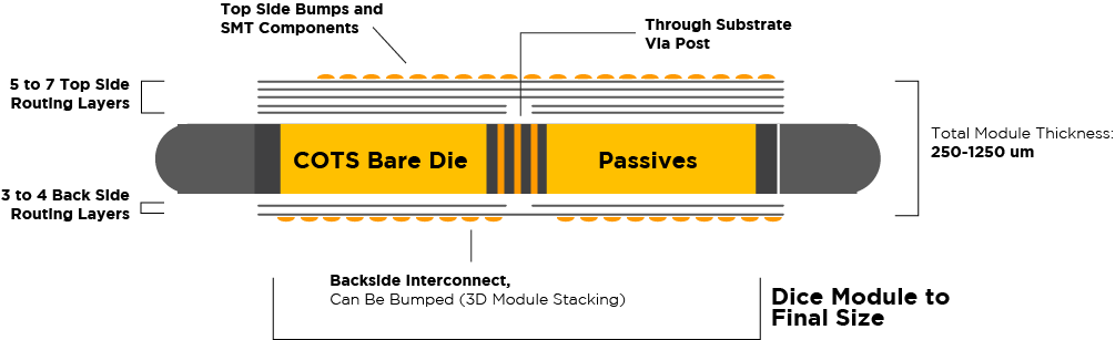
Without surface mounts
With surface mounts
SWaP and Benefits
Driving the largest reductions in Size, Weight and Power (SWaP)
Stacks as a subsystem – up to three slices
Scalable to larger wafer formats for future volume production demands
Embedded Die Interposer Technology
Can incorporate extracted/recovered die for faster prototyping and lower volume orders
Potential to connect all device technologies – MEMs, sensors, memory, analog, controllers etc.; and all source substrates: Si, GaAs, InP, glass devices – into one package
Uses TMV (Thru Mold Via) with no wire bonds or separate interposers
Up to 7 interconnect metal layers per side
Able to be brought out to BGA or SMT interfaces on both sides
Developed by Draper Laboratory for DoD applications, and HSiP is now available under license to i3 for wider DoD, commercial, or industrial uses
More robust system design than commercial off-the-shelf
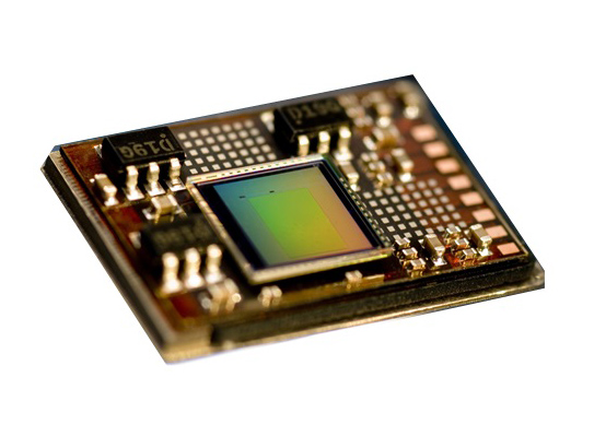
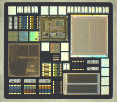
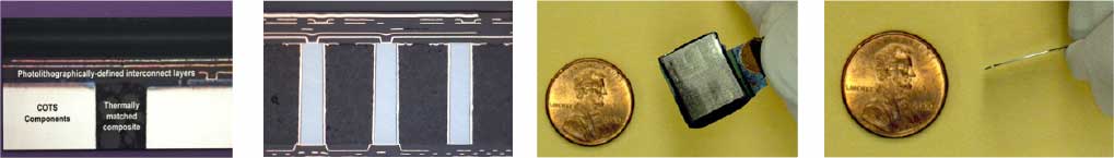
Typical highly-integrated digital HSIP module containing heterogeneous components
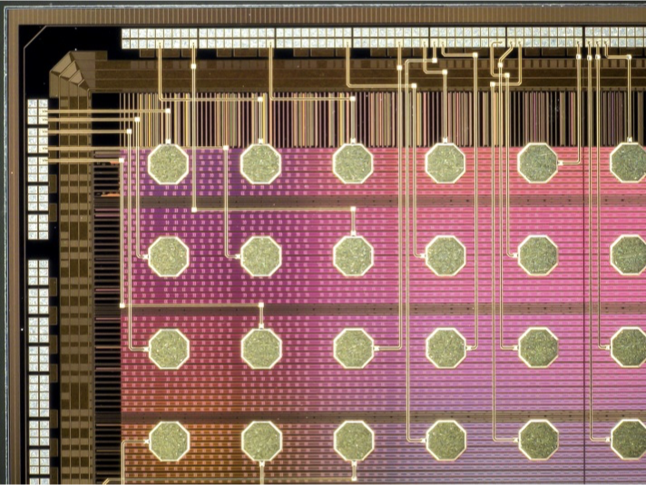
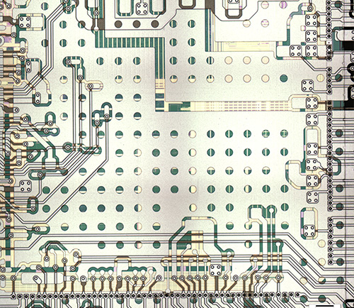
Typical Routing Layer in HSIP Technology
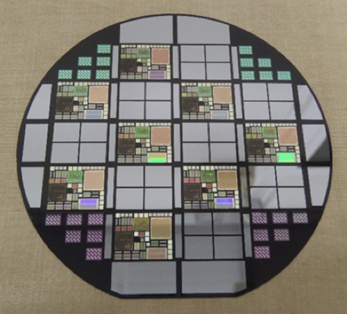
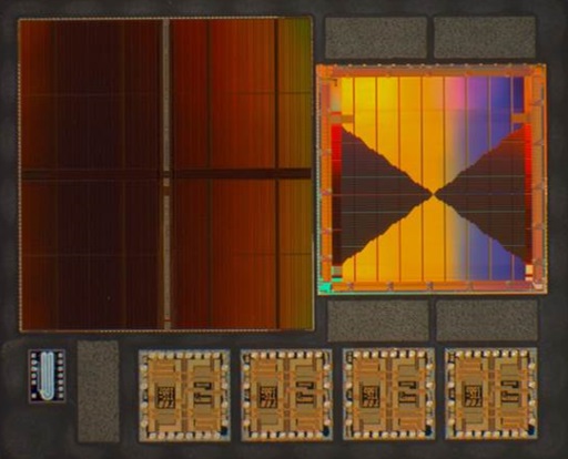
Typical completed HSiP wafer after 12 metal layers. 7 layers frontside, 5 layers backside.
Example of HSiP interconnect routing layers with nominal 18-micron lines, 25-micron via. The image is showing three routing layers.
Single Sub-Module Overview
Interconnect Fabric
Seven interconnect layers are possible on both the frontside and the backside, allowing for design possibilities such as controlled impedance transmission lines, power/ground bus, and signal line shielding for crosstalk isolation.
Multichip module, bare die, pre-interconnect
Multichip module, post-interconnect
3D Stacking with Heterogeneous MCMs
Individual Multichip Modules can be stacked for higher performance in the same footprint.